 Small batches, high standards. Our rapid prototyping service makes validation faster and easier —

Electroless Copper Plating: Avoid The Defects That Kill Yield
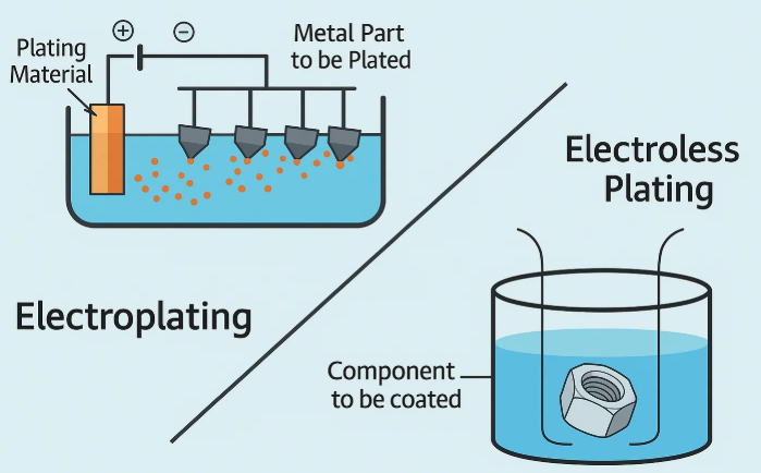
What Electroless Copper Plating Really Does
Electroless copper plating is a chemical deposition process that forms copper on a surface without an external power supply. Instead of using current to force metal onto a part, it relies on an autocatalytic reaction that begins on an activated surface. In manufacturing, that difference matters because geometry stops being the main obstacle to coverage. A ScienceDirect review highlights its ability to produce conformal thickness on complex shapes, and Wikipedia notes its common use on metals, plastics, and PCB through-holes.
What Is Electroless Copper Plating
Electroless copper plating deposits copper by chemical reduction on a catalytic surface, not by passing external current through the workpiece.
In plain terms, this is the copper plating route manufacturers use when they need an even, thin conductive layer in places that are difficult for current-driven methods to reach consistently. It is especially useful for through-holes, vias, recessed areas, and nonconductive materials that have been properly activated first.
How Electroless Plating Builds Copper Without Current
The bath supplies copper ions along with a reducing chemistry. Once the surface is catalytic, copper starts to deposit, and that newly formed copper helps the reaction continue. That self-sustaining behavior is why the process is called autocatalytic. Searchers sometimes type electron plating when they really mean this method or standard electroplating. In shop-floor language, electron plating is not the formal term. Electroless plating and electroplating are related to copper deposition, but they run on different mechanisms and demand different controls.
Why Uniform Copper Deposition Matters
Uniformity is the real advantage. In electrolytic processes, current density shifts across edges, recesses, and deep holes, so thickness can vary from one area to another. This method reduces that shape-driven imbalance, which is why it is widely used for PCB primary metallization and other parts with internal or irregular features. Engineers care because a more even starting layer supports conductivity continuity, adhesion, and later build-up steps. Buyers care because poor early coverage often turns into expensive defects much later.
- No external current is required during deposition.
- Coverage is more uniform on complex geometry and through-holes.
- Nonconductive surfaces can be metallized after activation.
- The process often creates the first conductive layer before thicker copper buildup.
- Stable results depend on chemistry, activation, and control, not just immersion time.
That last point carries most of the yield risk. When people assume electron plating is just a simple dip-and-coat step, they miss what really governs results: the surface must be prepared to start the reaction, and the bath must stay chemically balanced enough to keep copper growing evenly.
The Chemistry Behind a Stable Copper Plating Solution
Uniform coverage sounds simple, but the bath has to do two opposite jobs at once. It must hold copper ions in solution, then let them reduce only where deposition is supposed to happen. That is why a working copper plating solution is not just dissolved metal. It is a controlled chemical system built around copper supply, reduction, complexing, stabilization, alkalinity, and surface activation.
Main Components Of A Copper Plating Solution
When engineers ask about copper sulfate for plating, they are really asking about only one part of the recipe. Copper sulfate is widely used as the copper source in electroless baths, but the salt alone cannot produce a stable deposit. The bath also needs a reducing agent, usually an alkaline chemistry that can convert Cu2+ to metallic copper on a catalytic surface. Complexing agents keep copper soluble at high pH and strongly influence how fast the metal becomes available for deposition. Stabilizers and trace additives help prevent the solution from reducing copper in the tank instead of on the part.
| Bath component | Functional role | Why it matters on the part |
|---|---|---|
| Copper source | Supplies Cu2+ for deposition | Controls available metal for coverage and thickness build |
| Reducing agent | Chemically reduces copper at the catalytic surface | Drives deposition rate and affects gas generation and porosity risk |
| Complexing chemistry | Keeps copper soluble and moderates reactivity in alkaline solution | Influences initiation, deposit morphology, and bath stability |
| Stabilizers and additives | Suppress bulk decomposition, and in some cases fine-tune rate | Helps avoid roughness, particles, and uncontrolled plating |
| pH control | Sets reducer activity and copper speciation | Shifts plating rate, adhesion risk, and bath life |
| Activation chemistry | Creates catalytic sites before plating starts | Determines whether nonconductive or passive surfaces plate at all |
How Electroless Deposition Starts And Sustains
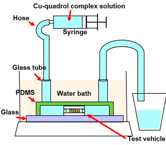
The reaction starts only where the surface is catalytic. On dielectrics and semiconductors, activation often uses stannous and palladium chemistry, as summarized by Taylor & Francis. On copper seed layers or already catalytic metals, initiation is more direct. Once the first copper nuclei form, the fresh deposit helps catalyze further reduction. That self-sustaining loop is the core of electroless deposition.
A recent Materials study shows how sensitive that loop can be. In a copper-quadrol bath, copper sulfate, formaldehyde, quadrol, cytosine, surfactant, temperature, and pH all shaped performance together. The researchers found pH had the strongest effect on decomposition time, while cytosine most strongly affected plating rate.
Why Bath Balance Controls Copper Coating Quality
Chemistry choices show up quickly in surface coverage and adhesion. Weak complexing leaves more free copper in solution, which raises the risk of particle formation and rough copper coating. Excessively aggressive pH, reducer activity, or temperature can speed deposition but shorten bath life and promote hydrogen bubbling. Too much stabilizer can do the opposite, slowing initiation and leaving thin or skipped areas on marginally activated features. Even the difference between a balanced bath and an unstable one can look small on a lab sheet, yet behave very differently on a real production line.
That is also where this process diverges from a copper electroplating solution. Here, the bath must create and control its own surface reaction without external current, so chemical balance directly governs morphology, continuity, and stability. In practice, the chemistry only performs as well as the sequence that prepares the surface for it.
How to Copper Plate
Chemistry only helps when the surface reaches the bath in the right condition. In production, many early copper failures are not mysterious bath events at all. They start with sequence mistakes, such as residue left in a drilled hole, weak conditioning, incomplete activation, or poor rinsing between tanks. If you are researching how to copper plate complex features reliably, this is the workflow that protects adhesion, coverage, and the next build step.
Cleaning And Surface Conditioning Before Copper Deposition
Published PCB process guides from ALLPCB and FastTurn describe a consistent front end: after drilling or handling, parts are cleaned, conditioned, and prepared before catalytic activation. The reason is simple. Copper will not start well on oil, fingerprints, oxides, resin smear, or drilling debris.
- Cleaning or de-oiling. Removes oils, dust, fingerprints, and shop residue. In PCB work, this also helps the hole wall accept later catalyst more evenly.
- Desmear or residue removal. For drilled boards, chemical cleaning removes resin smear and debris from via walls so the future conductive path is not blocked.
- Conditioning. A conditioner prepares the surface to adsorb catalyst more uniformly. This matters most on nonconductive or hard-to-wet surfaces.
- Micro-etch or surface preparation. On exposed copper, micro-etching removes light oxide and organic film while slightly roughening the surface for better bonding.
- Acid wash when required. Some PCB lines include an acid wash before catalyst steps to normalize the surface and reduce carryover.
The branch point appears here. Metals usually focus on oxide removal and surface readiness. Plastics need wetting and later catalytic seeding. PCB panels add drilled-hole cleaning because the hole wall contains insulating resin, not just copper foil.
Activation And Nucleation For Electroless Plating
Nothing deposits until catalytic sites exist. In PCB primary metallization, both references describe palladium-based activation as the trigger that allows copper reduction to begin on insulating hole walls. FastTurn also notes an acceleration step after colloidal palladium activation to expose the active palladium core more completely.
- Activation or catalysis. The surface receives catalytic species, commonly palladium chemistry in PCB applications, so deposition starts where it should.
- Acceleration. When colloidal palladium systems are used, this step removes surrounding compounds and improves catalyst activity.
- Initiation and nucleation. The first copper nuclei form at those active sites. Once a continuous film begins, the reaction becomes autocatalytic and continues on the fresh copper.
- Electroless deposition. The part enters the copper bath and builds a thin conductive seed layer. For PCB through-holes, process descriptions place this initial deposit at roughly 1 to 2 μm, or about 20 to 100 microinches, before later thickness buildup.
That is why many searches for copper plating how to guidance miss the real risk. People focus on the bath, but if the surface cannot hold catalyst, you cannot plate copper evenly, no matter how carefully the solution is maintained.
Rinsing Drying And Post Treatment Control
Plating copper cleanly depends just as much on what happens between wet steps as what happens inside the tank.
- Rinsing. Good rinsing limits chemical carryover that can contaminate the next bath, stain surfaces, or destabilize the deposit.
- Drying. Controlled drying helps prevent water marks, fresh-film oxidation, and handling damage.
- Post-treatment or handoff. In PCB manufacturing, the new conductive layer is usually the foundation for later electrolytic copper buildup. On other parts, post-treatment may center on inspection, adhesion checks, or protection before the next finish.
If you are deciding how to copper plate for yield, sequence discipline matters more than any single tank. A weak clean often shows up later as poor adhesion. Poor rinsing can look like random roughness. Inadequate activation can turn into skip plating. The logic stays the same across applications, but the preparation target changes with the substrate. Steel, stainless, aluminum, plastics, and drilled through-holes do not enter the line with the same surface condition, and that difference is where process flow becomes substrate strategy.
Copper Plating Steel, Aluminum, Plastic, and Stainless Prep
A part can move through the same line and still need a completely different start. That is where many yield losses begin. In electroless copper plating, the bath does not erase surface history. Steel, stainless steel, aluminum, plastics, and drilled dielectric features all arrive with different soils, oxides, wetting behavior, and activation needs. Pretreatment has to solve those differences before copper can form a continuous, adherent first layer.
How To Prepare Steel Stainless And Aluminum Surfaces
Metal parts already conduct electricity, but that does not mean they are ready to plate. For copper plating steel, the practical job is to remove shop oils, soils, and visible oxide so the surface is clean, wettable, and able to support adhesion. Copper plating stainless steel usually demands more care because the surface is protected by a passive film. Copper plating aluminum faces a similar issue, with an oxide layer that can interfere with bonding if preparation is weak or delayed. In all three cases, the real target is not a bright-looking part. It is an adhesion-ready surface with oxides reduced to the point that activation and initial copper deposition can proceed evenly.
This is why one generic metal-cleaning routine rarely works across every alloy. A line set up around mild steel logic may leave stainless or aluminum looking acceptable while still producing weak initiation, skip areas, or later blistering. Operators usually get better results when they match cleaning strength, oxide removal, and conditioning to the actual substrate rather than the tank label.
Why Copper Plating Plastic Requires Activation First
Copper plating plastic starts from the opposite problem. The substrate is not conductive at all. Sharretts describes a pretreatment path that can include cleaning, predip, etching, neutralizing, preactivation, activation, and acceleration before electroless deposition begins. The etch gives the surface better wetting and microscopic texture for adhesion. Activation adds catalytic sites. The first electroless deposit then creates an adherent metallic film that makes the part conductive for later buildup.
That sequence is why copper plating plastic cannot be treated like a dirty metal part that only needs degreasing. If etching is weak, the metal has little to grip. If sensitization or preactivation is poor, the activator may not distribute well. If activation is incomplete, the seed layer forms with gaps. The same logic applies to other nonconductive materials that need metallization before any current-driven plating step can work.
Preparation Logic For Through Holes And Nonconductive Features
PCB through-holes make this easier to visualize. Altium notes that primary metallization is performed after drilling and desmear to form a seed layer on the hole wall before later copper build-up. Even though copper foil exists on the board surface, the dielectric wall inside the hole still needs reliable activation and a continuous initial deposit. If that seed layer is discontinuous, later plating cannot rescue the missing path cleanly.
Deep recesses, blind features, and mixed-material parts follow the same rule. Preparation must reach the actual area that needs copper, not just the easiest area to inspect.
| Substrate type | Preparation goal | Key risks | What the process must accomplish |
|---|---|---|---|
| Steel | Remove oils and oxide, create a clean active surface | Residual soil, rust, poor wetting | Support uniform initiation and good adhesion |
| Stainless steel | Condition a passive surface for activation | Persistent passive film, weak bonding | Make the surface plateable rather than merely clean |
| Aluminum | Control oxide before deposition begins | Rapid oxide re-formation, adhesion loss | Create a stable, activation-ready surface |
| Plastics such as ABS | Etch, activate, and create a conductive seed layer | No conductivity, poor wetting, low mechanical keying | Turn a nonconductive surface into a reliably metallized one |
| PCB through-holes and dielectric features | Desmear and metallize the feature wall | Missed activation, discontinuous seed coverage | Form a continuous base for later copper build |
Substrate strategy decides whether the bath gets a fair chance. After that, consistency lives or dies on operating control: temperature, pH, contamination, loading, agitation, and rinsing discipline all determine whether a well-prepared surface stays defect-free through the rest of the line.
Cu Plating Variables That Affect Later Build
Pretreatment gets the surface ready. Stable operation keeps it ready long enough to matter. In real production, a good electroless copper line is not just a chemistry setup. It is a control system. Michael Carano's I-Connect007 guide describes these baths as thermodynamically unstable by nature, which is why small shifts in operating conditions can turn into copper loss, plate-out, excess stress, or inconsistent deposition.
Process Variables That Control Cu Plating Consistency
Operators usually see the problem first as drift, not disaster. Bath age shows up through by-product buildup. In Carano's discussion, formate, carbonate, and chloride accumulate over time, and rising specific gravity is used as a practical warning sign. Temperature matters too. Higher heat improves activity but reduces stability, while very low temperature can sacrifice deposition rate. Overall chemistry balance matters just as much. When the bath runs out of chemistry specification, the reducing system becomes less predictable, which affects coverage, stress, and tank life.
Contamination control is another quiet yield killer. Poor rinsing lets organics, inorganics, and catalyst residues enter the tank. Carano specifically warns that palladium drag-in can trigger instantaneous decomposition. Agitation, filtration, and loading round out the picture. Filtration has to remove copper particles effectively. Low loading with intermittent use can reduce active stabilizer and increase copper loss. That is why process control for cu plating is really a discipline of trend monitoring, not occasional troubleshooting.
| Variable | Why it matters | Likely symptoms when out of control | Downstream manufacturing effect |
|---|---|---|---|
| Bath age and specific gravity | Tracks by-product buildup and rising instability | Copper dust, plate-out, excessive thickness, stressed deposit | Weak seed layer, higher blistering risk, more variation in later copper build |
| Temperature | Changes stability and deposition rate | Sudden instability at the high side, slow coverage at the low side | Uneven base thickness and inconsistent handoff to later plating steps |
| Chemistry balance, including pH and reducer condition | Controls how cleanly copper reduces at the surface | Slow deposition, skip areas, random decomposition | Poor continuity and unreliable conductivity for subsequent buildup |
| Copper availability | Determines whether features receive a continuous initial film | Thin deposit, delayed initiation, uneven appearance | Weak foundation for thickness build or finishing quality |
| Contamination and drag-in | Foreign material destabilizes the bath and seeds roughness | Particles, roughness, rapid decomposition | Nodules, adhesion loss, rough overplated surface |
| Agitation and filtration | Keep chemistry uniform and remove copper particles | Localized variation, particulate roughness, sludge buildup | Defects telegraph into later layers and reduce finishing consistency |
| Loading and rinsing discipline | Affect stabilizer activity, drag-in, and repeatability | Panel-to-panel variation, excessive copper loss after idle time | Harder process window in volume production and lower yield repeatability |
How Deposit Quality Affects Plating On Copper Later
The first layer is rarely the last layer. If the initial plated copper is thin, rough, porous, or highly stressed, later plating on copper tends to magnify the weakness instead of fixing it. Carano notes that deposit stress can contribute to blistering from the hole wall and separation from the internal layer copper interface. In finishing applications, an acid copper review shows that later copper build is often expected to add thickness, leveling, and brightness. That only works when the base deposit is continuous and adherent.
For engineers, that means early electroless quality affects more than coverage. It influences later copper buildup, adhesion to following layers, surface smoothness, and how consistently the part carries current or accepts a finish. For buyers, the message is simpler: a cheap-looking seed problem often becomes an expensive assembly or reliability problem.
What Operators Should Watch Before Defects Multiply
The warning signs are usually easy to overlook. Trend specific gravity each shift. Watch for unusual copper dust, more particles in the filters, longer time to coverage, random roughness after idle periods, or instability shortly after catalyst-heavy work moves through the line. Those clues often point upstream to loading, rinsing, contamination, or bath age before visible defects become widespread.
- Track shift-by-shift trends, not just pass or fail checks.
- Audit rinse quality and drag-in points around activation and acceleration steps.
- Link first defects to idle time, maintenance events, and bath turnover history.
That distinction becomes important when the process plan is being chosen. Some jobs need the uniform seed layer this method provides in holes, recesses, or nonconductive areas. Others care more about how fast thickness can be built once conductivity already exists.
Electroplating vs Electroless Plating in Real Manufacturing
The right process choice usually comes down to one question: do you need reliable first coverage, or do you need fast copper buildup? In many manufacturing lines, electroless copper plating is used first because it can deposit on activated nonconductive surfaces and coat difficult features evenly. In PCB fabrication, ALLPCB describes it as the thin conductive seed that makes later electrolytic buildup possible.
Best Uses For Electroless Copper In Manufacturing
This process fits parts where geometry makes current distribution unreliable. Typical examples include PCB primary metallization, through-hole walls, blind or recessed features, and plastics or ceramics that must be metallized before any current-driven step can begin. Because deposition is autocatalytic rather than electrical, it gives more conformal coverage on complex internal shapes. For teams weighing electroplating vs electroless plating, that uniformity is the real advantage, especially when continuity matters more than speed.
When Copper Electroplating Becomes The Better Next Step
Once a conductive path already exists, copper electroplating is usually the stronger choice for thickness, throughput, and later-stage conductor build. Both Aivon and ALLPCB note that electrolytic deposition builds copper faster and is commonly used after the chemical seed layer. In plain shop terms, electroless starts the surface, while electroplating copper builds the mass. If the goal is electroplating with copper for thicker traces, stronger via walls, or higher-volume production, an electrochemical plating step is often the better fit. In hybrid PCB flow, the thin seed is followed by a thicker copper electroplate.
How To Decide Between Uniform Coverage And Faster Build
| Application need | Better process fit | Strengths | Limitations | Typical workflow position |
|---|---|---|---|---|
| PCB through-holes and primary metallization | Electroless | Seeds insulating hole walls uniformly | Thin deposit, slower buildup | First conductive layer before bulk copper |
| Plastic, ceramic, and other nonconductive substrates | Electroless | Can plate activated nonconductive surfaces | Requires careful pretreatment and activation | Initial metallization step |
| Complex recesses and high-aspect-ratio features | Electroless | Less affected by current distribution problems | Not ideal for rapid thick buildup | Uniform seed or thin functional layer |
| Existing conductive surfaces needing thickness | Electrolytic | Faster deposition and controllable bulk build | Needs a conductive base and good current control | Second-stage thickness build |
| High-volume standard conductive parts | Electrolytic | Better throughput for production | Can plate unevenly in difficult geometry | Main conductor buildup step |
People searching for electroplating with copper are often comparing two tools that work best together, not always against each other. The costly mistakes appear when one method is forced to do a job it was not designed for. Thin coverage in recesses, voids in difficult holes, or wasted cycle time in bulk buildup often trace back to that mismatch, which is why defect analysis has to look at process fit as closely as bath condition.
Copper Electroless Plating Defects and Troubleshooting Guide
Yield loss usually announces itself with a visible flaw, not a lab report. In copper electroless plating, that first clue might be a skip area in a hole wall, a blister after thermal stress, or random nodules that seem to appear overnight. The trap is assuming the defect started where it became visible. Some problems are first noticed after a downstream electroplating bath, even though the real failure began earlier in cleaning, activation, rinsing, or bath control. I-Connect007 notes that electroless copper solutions are thermodynamically unstable by nature, which is why defect diagnosis has to combine surface history with tank stability.
How To Read Common Copper Electroless Plating Defects
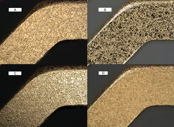
Many visible plating defects begin upstream in preparation or control, not during deposition alone.
Read each defect by three clues: where it appears, what it looks like, and when it shows up. A flaw concentrated in through-holes or recesses usually points to wetting, activation, or gas-release problems. A random defect spread across surfaces often points to contamination, copper dust, or filtration issues. A blister that appears only after later processing suggests weak adhesion or deposit stress rather than simple appearance loss. Guidance from PCBWay and Chem Research reinforces the same shop-floor lesson: poor cleaning, incomplete rinsing, and contaminated solutions can all show up later as bad copper deposition.
| Symptom | Probable causes | Verification checks | Corrective actions |
|---|---|---|---|
| Skip plating | Weak cleaning, poor activation, trapped air, low bath activity, poor coverage in recesses | See if defects cluster in holes, corners, or low-flow areas; compare flat surfaces to recessed features | Audit pretreatment and activation, improve wetting and agitation, confirm chemistry and temperature |
| Poor adhesion or blistering | Oil, oxide, inadequate micro-etch, contaminated substrate, stressed deposit, unstable bath | Look for peeling after handling or heat exposure; inspect whether failure is at the substrate interface | Strengthen cleaning and oxide removal, renew pretreatment solutions, reduce bath instability and deposit stress |
| Roughness | Particles, organic contamination, copper dust, poor filtration, plate-out fragments | Check filters, tank walls, and heaters for solids or loose copper; inspect whether texture is random and raised | Improve filtration, remove debris sources, clean tank hardware, correct contamination before more parts run |
| Pitting | Air bubbles, particles, residues, poor agitation, poor rinsing carryover | Identify crater-like defects, especially in recessed or low-flow zones | Improve agitation and rinsing, reduce drag-in, filter the bath, review part orientation |
| Voiding in holes or features | Incomplete desmear, weak conditioning, poor catalyst coverage, blocked hole walls, discontinuous initiation | Cross-section or continuity check; compare surface deposit to hole-wall coverage | Recheck drilled-hole preparation, activation uniformity, rinsing discipline, and feature wetting |
| Slow deposition | Low temperature, bath age, by-product buildup, chemistry drift, marginal activation | Longer time to visible coverage, thin deposits on both coupons and production parts | Review operating temperature, restore chemistry, refresh aged solution as needed, confirm activation quality |
| Nodules | Copper particles in solution, decomposition, poor filtration, tank plate-out breaking loose | Look for isolated bumps and increased particle loading in filters | Clean the system, improve particle removal, inspect for plate-out on tank surfaces and heaters |
| Discoloration or dull appearance | Contamination, breakdown products, poor post-rinsing, drying residues | Compare fresh-run parts to end-of-run parts; inspect for residue after rinse and dry | Improve rinsing and drainage, reduce contamination sources, refresh solution if by-products are building up |
| Bath instability or plate-out | High specific gravity, higher temperature, by-product buildup, poor filtration, palladium drag-in, extended idle or low loading conditions | Watch for copper loss, dust, fast filter loading, or copper on tank walls and heaters | Trend specific gravity each shift, control temperature, improve rinsing before entry, maintain filtration, and perform partial bath refresh or tank maintenance as needed |
Root Causes Hidden In The Copper Plating Solution
Several high-cost defects start inside the tank long before the finish looks bad. Carano's electroless copper discussion shows that stability falls as specific gravity increases, and it also falls as temperature rises. He also notes that specific gravity should be monitored each shift because by-products such as formate, carbonate, and chloride build up as the bath ages. That buildup increases the chance of copper loss, plate-out, and unstable copper deposition. Filtration matters just as much. If copper particles are not removed effectively, roughness and nodules become much more likely.
Contamination does not need much time to do damage. PCBWay emphasizes that poor washing after oil removal and charge-adjustment steps can carry pollutants forward. Carano adds a sharper warning for PCB lines: palladium drag-in can cause instantaneous solution decomposition. When a bath starts behaving unpredictably, the visible defect may change from run to run, but the root cause is often the same drift in cleanliness, chemistry, or maintenance discipline.
Corrective Actions Before The Bath Drifts Further
Start with fast checks that separate a surface problem from a solution problem.
- Map the defect location. Localized failures usually point to pretreatment, activation, or trapped air.
- Inspect filters, heaters, and tank walls for copper plate-out or loose particles.
- Review specific gravity, temperature, loading history, and idle time together, not one by one.
- Audit rinse performance before the electroless tank, especially after catalyst and accelerator stages.
- Use cross-sections or continuity checks when holes look suspicious but surfaces appear acceptable.
If the problem is widespread, resist the urge to blame only the workpiece. If it follows certain features or materials, resist the urge to blame only the bath. Reliable troubleshooting sits in the overlap between preparation, activation, and solution control. That same overlap is where production teams decide whether a line is merely able to plate sample parts or truly ready for repeatable release into larger manufacturing programs.
From Sample Electroless Copper Plating to Production
Finding the root cause is only half the battle. Launch risk appears when a line that can make a few good samples has to hold the same result across pilot lots, documentation reviews, and full production demand. For buyers sourcing electroless copper plating, the real question is not simply whether a shop can make a copper plated part. It is whether that supplier can prove repeatability on your substrate, geometry, and downstream process.
What Buyers Should Validate Before Production Release
Automotive sourcing usually asks for more than visual acceptance. American Electro highlights IATF 16949, ISO 9001, and APQP discipline for automotive suppliers, while PPAP guidance frames Production Part Approval Process requirements as the proof that parts and processes are ready for mass production. That matters whether you are qualifying copper plating metal brackets, a copper plated plastic housing, or a mixed-material assembly.
- Match the approved process flow to the real manufacturing route, including cleaning, activation, deposition, rinse, dry, inspection, and any later copper build or copper superfinish.
- Ask for PFMEA, control plans, and acceptance criteria tied to plating risks such as skip coverage, adhesion loss, and thickness variation.
- Confirm how thickness and adhesion are measured. A sound MSA or Gage R&R matters as much as the nominal plating spec.
- Define the PPAP submission level early, including whether PSW-only documentation is enough or a fuller package is required.
- Request material performance evidence for the actual use case, especially if the copper plated part will be formed, soldered, assembled, or finished later.
How Surface Treatment Fits Into End To End Part Manufacturing
Surface treatment is rarely a standalone purchase. It sits inside a chain that may include stamping, CNC machining, deburring, cleaning, plating, inspection, packaging, and traceability. That is why supplier selection should look beyond the tank line itself. A partner with stronger end-to-end control can reduce handoff errors because burr condition, surface cleanliness, and part handling are managed with plating in mind. This becomes especially valuable when a copper plated feature must support later assembly or a specified copper superfinish.
When To Engage A Qualified Automotive Supplier
If the program carries launch, warranty, or safety risk, involve a qualified automotive supplier early. One practical example is Shaoyi, which offers stamping, CNC machining, custom surface treatment, prototyping, and volume production under IATF 16949. That kind of broader capability can simplify evaluation when you want fewer supplier handoffs. Still, the better test is a disciplined checklist:
- Can the supplier support prototype, pilot, and volume production without quietly changing the core process?
- Do lot records connect plating results to traceability, inspections, and corrective actions?
- Can they explain how they manage substrate differences, including copper plating metal parts versus copper plated plastic components?
- Will they provide the quality package your customer actually needs, from process flow charts to PSW?
The strongest sourcing decisions sit where chemistry control meets manufacturing discipline. That is where plating quality stops being a sample result and becomes supply-chain reliability.
Electroless Copper Plating FAQs
1. What is electroless copper plating and how is it different from electroplating?
Electroless copper plating is a chemical process that deposits copper without an external power source. It starts on a properly activated surface and keeps building through an autocatalytic reaction. Electroplating, by contrast, depends on electric current, so thickness can vary more across edges, recesses, and deep features. In practice, electroless copper is often chosen for the first conductive layer, while electroplating is used later for faster thickness buildup.
2. Can electroless copper plating be used on plastic and other nonconductive materials?
Yes, but only after the surface is prepared to accept the reaction. Nonconductive parts usually need cleaning, etching, activation, and a catalytic seed before copper can form evenly. That is why the pretreatment route matters as much as the plating bath itself. This approach is widely used for plastic components, PCB hole walls, and other surfaces that cannot be plated directly by current-driven methods at the start.
3. What are the most common causes of skip plating or poor adhesion?
The most common causes are weak cleaning, incomplete oxide removal, poor activation, trapped air in difficult features, and bath imbalance. Many shops first blame the copper bath, but the real issue often begins earlier in rinsing or pretreatment. Clues such as defects concentrated in holes, corners, or mixed-material areas usually point to surface preparation problems. Widespread roughness or random nodules more often suggest contamination, particles, or instability in the solution.
4. When should electroless copper be used before copper electroplating?
It is usually the better first step when a part needs uniform coverage in through-holes, recesses, or activated nonconductive areas. Once that thin conductive layer is in place, copper electroplating often becomes the more efficient option for building thickness. This two-step flow is common in PCB manufacturing and other applications where coverage quality matters before bulk deposition speed. Choosing the wrong sequence can increase voids, weak adhesion, and later reliability issues.
5. What should buyers verify before approving a supplier for production electroless copper plating?
Buyers should check more than sample appearance. A strong supplier should show control of pretreatment, activation, rinsing, bath monitoring, inspection, and traceability across pilot and production lots. It also helps to confirm whether the supplier can support the full manufacturing route, including machining or stamping before plating and quality documentation after plating. For automotive programs, an integrated partner such as Shaoyi can be a useful benchmark because it combines metal part manufacturing, surface treatment, prototyping, and volume production under IATF 16949, but the key test is still process control and repeatability on your exact part.